Login Department of Materials Engineering and Science, National Gormosa University

使用自然人憑證登入
Forgot your password?
  • Orbit Logo

    please login to manage web,click to open login window

  • home

Department of Materials Engineering and Science, National Gormosa University

::: Home NFU Sitemap

Department of Materials Engineering and Science, National Gormosa University Logo Department of Materials Engineering and Science, National Gormosa University

:::
  • Introduction
    • Introduction
    • Establishment history
    • Educational objectives & Core ability
    • Current Situation of Academic System
    • Previous Head of Department
    • Department administrative Organization
    • Department Building Configuration Diagram
  • News
  • Faculty
    • Full-time teachers
    • Part-time teacher
    • Retired teacher
    • Administrative team
  • Courses
    • Graduation standards at all levels
    • Regulations
    • Course Map
  • Equipment
    • Experiment Apparatus
    • List of laboratory instructors
    • Laboratory of Scanning Electron Microscopy
    • Transmission Electron Microscopy Lab
    • Laboratory of X-ray Diffraction
    • Metallurgy Laboratory
    • Laboratory of Mechanical Properties
    • Metallographic Laboratory
    • Laboratory of Precision Casting
    • Semiconductor Process Laboratory
    • Laboratory of Heat Treatment
    • Non-Destructive Testing Laboratory
    • Polymer Processing Laboratory
    • General Workshop
    • Materials Analysis Laboratory
    • College of Management(Dept. of Materials)
    • Additive Manufacturing Laboratory
  • Students
  • Enrollment
    • Admissions Information
    • Smart Foundry Industry–Academia Cooperative Program
    • Admission Gallery
  • Download
  • Association
    • Student Association
    • Department of Materials Science and Engineering Alumni Association
    • Event Gallery
  • Contact Us
Experiment Apparatus
    • 繼續播放

      暫停播放

    :::

    Facility

    • Experiment Apparatus
      • List of laboratory instructors
        • Laboratory of Scanning Electron Microscopy
          • Transmission Electron Microscopy Lab
            • Laboratory of X-ray Diffraction
              • Metallurgy Laboratory
                • Laboratory of Mechanical Properties
                  • Metallographic Laboratory
                    • Laboratory of Precision Casting
                      • Semiconductor Process Laboratory
                        • Laboratory of Heat Treatment
                          • Non-Destructive Testing Laboratory
                            • Polymer Processing Laboratory
                              • General Workshop
                                • Materials Analysis Laboratory
                                  • College of Management(Dept. of Materials)
                                    • Additive Manufacturing Laboratory
                                      • Home
                                      • Equipment
                                      • Experiment Apparatus

                                      Experiment Apparatus

                                      The department was established when the school was founded in 1989 and was renamed as the Department of Materials Science and Engineering in 1989. The purpose is to cultivate talents with materials research, material analysis, material processing, and material processing. The main teaching goal is to cultivate talents required by the domestic cutting-edge materials industry and the application of the optoelectronic semiconductor industry. The faculty of the department is strong, the teaching is lively and lively, and the curriculum design focuses on application and in line with the trend of the times.

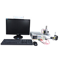
                                      experiment apparatus

                                      The department was established when the school was founded in 1989 and was renamed as the Department of Materials Science and Engineering in 1989. The purpose is to cultivate talents with materials research, material analysis, material processing, and material processing. The main teaching goal is to cultivate talents required by the domestic cutting-edge materials industry and the application of the optoelectronic semiconductor industry. The faculty of the department is strong, the teaching is lively and lively, and the curriculum design focuses on application and in line with the trend of the times.
                                      Share
                                      Tweet
                                      Print this page

                                      National Formosa University
                                      Department of Materials Engineering and Science

                                      Address : 632, No. 64 Wenhua Road, Huwei Town, Yunlin Count
                                      TEL : +886-5-631-5461FAX : +886-5-636-1981 E-mail:
                                      Copyright © Department Materials Science and Engineering, National Formosa University. All Rights Reserved. 
                                      Ruling DigitalVisits : 35802